lithography
US
・UK
A1 初級
n. (u.)不可數名詞石版印刷術
It is necessary for an artist to practice for years to become skilled in the technique of lithography
影片字幕

ASML 新款 4 億美元高數值孔徑機臺如何讓晶片跑更快! (How ASML Makes Chips Faster With Its New $400 Million High NA Machine)

- We're here at ASML's headquarters in the Netherlands, where 100% of the world's extreme ultraviolet lithography machines are made.
我們這裡是 ASML 位於荷蘭的總部,全球 100% 的極紫外光刻設備都是在這裡製造的。
- We're here at ASML's headquarters in the Netherlands, where 100% of the world's extreme ultraviolet lithography machines are made,
我們這裡是 ASML 位於荷蘭的總部,全球 100% 的極紫外光刻設備都是在這裡製造的。
史丹佛奈米製造實驗室:乾蝕刻介紹 (共 4 部,第 1 部) (Stanford Nanofabrication Facility: Dry Etching - Introduction (Part 1 of 4))
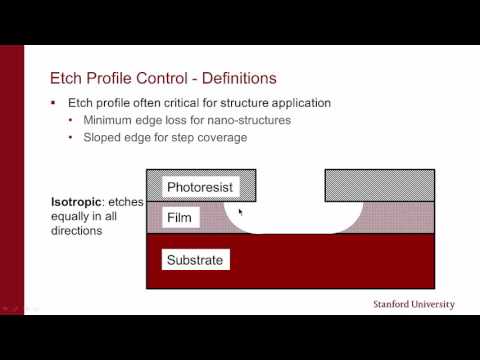
- Two of the other major processes used in nanofabrication, deposition, the process of laying down films, and lithography, the process of patterning the matte, usually films of fold resist, will be covered in other units of this course.
本課程的其他單元還將介紹納米制造中使用的其他兩個主要工藝,即沉積(鋪膜工藝)和光刻(圖案化亞光(通常是摺疊抗蝕劑薄膜)工藝)。
- and lithography, the process of patterning the match, usually films of photoresists—will be covered in other units of this course.
是以,揮發性副產品對於幹法蝕刻至關重要。
晶片荒衝擊生活!CNBC Beyond The Valley 深度剖析 (The global chip shortage will probably hit your everyday life | CNBC Beyond The Valley)
- A good example is ASML over in the Netherlands making that extreme ultraviolet lithography machine.
但這確實是解決危機的最佳槓桿,比我們目前認為的要快。
- So for example, ASML in lithography, ASMI in atomic layer deposition.
而這些芯片每兩年設計一次,以摩爾定律的事件為神奇,然後
西方國家陷入危機! (The West is in Trouble)
- If not for American companies pioneering AI, if not for Dutch companies building ultra-lithography technology that makes the chips possible, or British companies developing advanced jet engines, heck for all the bluster and scare-mongering, the West still does some pretty incredible mind-boggling things.
我住在南倫敦的祖父母家,就在協和號的航道正下方。
- If not for American companies pioneering AI, not for Dutch companies building ultra lithography technology that makes the chips possible.
如果不是美國公司開創了 AI,也不是荷蘭公司建造了讓晶片成為可能的極紫外光刻技術。
全球晶圓代工廠如何引領兆元晶片大戰! (How GlobalFoundries Is Steering the Trillion Dollar Chip Race)
- So lithography is the area that people talk about the most as the most expensive.
так, литография — это область, о которой люди больше всего говорят как о самой дорогой.
- So lithography is the area that people talk about the most as the most expensive.
是以,你會看到這些極度精密且非常昂貴的曝光機臺。
臺積電亞利桑那新廠!蘋果終於要在美國生產先進晶片了! (TSMC’s New Arizona Fab! Apple Will Finally Make Advanced Chips In The U.S.)

- The only machines in the world able to perform the extreme ultraviolet lithography necessary for etching minuscule designs on the most advanced chips.
這是世界上唯一能夠執行極紫外光刻的機器,這對於在最先進的晶片上蝕刻微小圖案是必要的。
- The fab is filled with billions of dollars of machinery operating at the very edge of what's scientifically possible, like these bus-sized EUV machines made by a single company, ASML, the only machines in the world able to perform the extreme ultraviolet lithography necessary for etching minuscule designs on the most advanced chips.
我們說的是規模龐大。
iPhone 徹底改變了 RF 濾波器! (The iPhone Forever Changed the RF Filter)
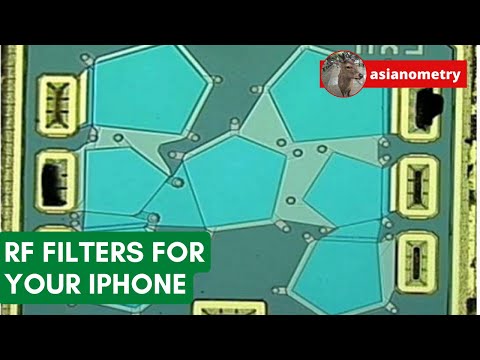
- After that, we use lithography to pattern the filter's features onto that metal layer.
我們應該花點時間討論一下這些系統是如何製造的。
- After that, we use lithography to pattern the filter's features onto that metal layer.
之後,我們用微影技術在金屬層上製作濾波器的特徵。
為什麼臺灣生產了所有「嗶嗶」叫的晶片? (Why Taiwan Makes All The Chips That Beep Boop)
- Like these machines, extreme ultraviolet lithography machines.
與這些機器一樣,極紫外線光刻機也是如此。
- Like... these machines—Extreme Ultraviolet Lithography Machines.
這些工廠的工藝從 500 納米到 3 納米不等,其中 5 個位於新竹科學園區,3 個位於臺南的臺灣南部科學園區,包括目前世界上最好的工廠,1 個位於臺中的臺灣中部科學園區,2 個位於中國,1 個位於上海,另一個位於南京、最後在美國,一座位於華盛頓州卡馬斯,一座位於鳳凰城,包括 6 座在建晶圓廠。
【國際議題】剛贏得美國大選的川普很快將面臨一場輸不起的對華關稅戰 (Trump Is Facing a Losing Tariff War With China)
- Massive appliances like these extreme ultraviolet lithography machines, developed by Dutch company ASML.
像這些由荷蘭 ASML 公司開發的極紫外線光刻機這樣的大型設備。
- Massive appliances like these extreme ultraviolet lithography machines developed by Dutch company ASML.
當習近平主席將某件事列為中國的優先事項時,他可以指著銀行提供廉價融資。