
after all
US /ˈæftɚ ɔl/
UK /ˈɑ:ftə ɔ:l/
- adv.畢竟;終究;到底;到底;終究;無論如何;別忘了;要知道
- phr.畢竟;終究;終究;終究
B1 中級更多alignment
US /əˈlaɪnmənt/
UK /əˈlaɪnmənt/
- n.結盟;對齊
B2 中高級更多as well as
US /æz wɛl æz/
UK /æz wel æz/
- adv.以及
- prep.以及
- conj.和…一樣好
A1 初級更多assemble
US /əˈsɛmbəl/
UK /əˈsembl/
- v.t.集合
- v.t./i.集合;聚集
B1 中級多益中級英檢更多audio
US /ˈɔ:dioʊ/
UK /ˈɔ:diəʊ/
- adj.音頻
- n. (u.)音訊;聲音
- n.音響設備;錄音;音響系統
B2 中高級多益中級英檢更多bundle
US /ˈbʌndl/
UK /ˈbʌndl/
- n. (c.)捆;束;大堆;大批
- v.t.捆綁;(電腦軟體等的)捆綁銷售;搭售;匆匆送走
B1 中級更多cardboard
US /ˈkɑ:rdbɔ:rd/
UK /ˈkɑ:dbɔ:d/
- n. (u.)硬紙板
B1 中級高級英檢更多chip
US /tʃɪp/
UK /tʃɪp/
- v.t.刮去;鑿去;挑球
- n. (c./u.)碎屑;芯片;晶片;炸薯條(英國)(美國)薯片;輕擊短打
B1 中級中級英檢更多coat
US /koʊt/
UK /kəʊt/
- n.夾克
- v.t.塗漆;鍍
A2 初級初級英檢更多component
US /kəmˈponənt/
UK /kəmˈpəʊnənt/
- n. (c./u.)構成部分;要素;成分;(電子)元件;分量;分力;(電腦)組件
- adj.零件
A2 初級高級英檢更多connectivity
US /ˌkɑnɛkˈtɪvɪti/
UK /ˌkɒnekˈtɪvɪti/
- n. (u.)連通性
B1 中級更多definitive
US /dɪˈfɪnɪtɪv/
UK /dɪˈfɪnətɪv/
- adj.決定性的;決定性的
B2 中高級高級英檢更多depth
US /dɛpθ/
UK /depθ/
- n.深;深度
A2 初級中級英檢更多electrical
US /ɪˈlektrɪkl/
UK /ɪˈlektrɪkl/
- adj.電的 ; 有關電的;有電工技能的;電器工業的;觸電的
A2 初級中級英檢更多electrically
US /ɪˈlɛktrɪklɪ/
UK /ɪ'lektrɪklɪ/
- adv.電地 ; 有關電地
A2 初級更多ensure
US /ɛnˈʃʊr/
UK /ɪn'ʃʊə(r)/
- v.t.保證 ; 確保
A2 初級多益中級英檢更多factory
US /ˈfæktəri/
UK /ˈfæktri/
- n. (c.)製造廠 ; 工廠
A2 初級多益初級英檢更多flat
US /flæt/
UK /flæt/
- n. (c./u.)公寓;(某物的)平面部分;降調;平底鞋
- v.t./i.合租;失敗
- adv.斷然地;固定不動地
- adj.平整;沒有活力的;洩氣的;走了氣的;固定的;無光澤的;平淡的;平面的
A2 初級初級英檢更多from A to Z
US /frʌm eɪ tə zi/
UK /frɒm eɪ tə zed/
- idm.從頭到尾
B2 中高級更多in depth
US /ɪn dɛpθ/
UK /in depθ/
- adv.深入地
insert
US /ɪnˈsɜ:rt/
UK /ɪnˈsɜ:t/
- v.t.插進 ; 嵌入 ; 插入;添加文字;(電腦)插入
- n.插;(雜誌)插頁
B1 中級多益中級英檢更多insertion
US /ɪnˈsə:ʃən/
UK /ɪn'sɜ:ʃn/
- n. (u.)插入 ; 刊載 ; 插入物
B1 中級更多inspection
US /ɪnˈspɛkʃən/
UK /ɪnˈspekʃn/
- n.調查 ; 檢查
B1 中級多益高級英檢更多made with
US
UK
- phr.用...製成;以...製作;帶有...情感
- phr. v.提供
A1 初級更多major
US /ˈmedʒɚ/
UK /'meɪdʒə(r)/
- n. (c.)陸軍少校;主要專業;;成年人
- adj.大聯盟;最重要的;一個主要;較大的;主要的;大調的
- v.i.到主要
A2 初級多益初級英檢更多manual
US /ˈmænjuəl/
UK /ˈmænjuəl/
- adj.手動;手動車
- n. (c.)手冊;說明書
A2 初級多益中級英檢更多manually
US /ˈmænjʊəlɪ/
UK /'mænjʊəlɪ/
- adv.手工製作;手動
A2 初級多益更多misplace
US /ˌmɪs'pleɪs/
UK /ˌmɪsˈpleɪs/
- v.t.誤放;誤給;遺忘;忘記將…放置何處
C2 高級更多motherboard
US /ˈmʌðərbɔ:rd/
UK /ˈmʌðəbɔ:d/
- n.母板;主機板
C2 高級更多mount
US /maʊnt/
UK /maʊnt/
- v.t.鑲嵌;裱貼;鑲嵌;舉行;舉辦(活動);發動(攻擊)
- n.底座;馬
- v.i.騎上(馬或腳踏車);登上;爬上
- prop. n.山;峰
B2 中高級高級英檢更多off of
US /ɔf ʌv/
UK /ɔf ɔv/
- prep.從...離開
A1 初級更多oven
US /ˈʌvən/
UK /ˈʌvn/
- n.烤箱
B1 中級初級英檢更多paste
US /pest/
UK /peɪst/
- v.t.貼上;粘貼中
- n. (c./u.)糊;漿糊;麵團
B1 中級初級英檢更多process
US /ˈprɑsˌɛs, ˈproˌsɛs/
UK /prə'ses/
- v.t.用電腦處理(資料);(依照規定程序)處理;處理;流程;加工;理解
- n. (c./u.)(規定的)程序;過程;進程;方法;法律程序;進程
A2 初級多益中級英檢更多quality
US /ˈkwɑlɪti/
UK /'kwɒlətɪ/
- n. (c./u.)質量;品質;質量;社會地位
- adj.優質的
A2 初級多益初級英檢更多ram
US /ræm/
UK /ræm/
- n.撞錘;公羊 ; 撞槌;隨機存取記憶體
- v.t.猛撞,猛擊;塞進
B1 中級更多recognise
US /'rekəgnaɪz/
UK /'rekəgnaɪz/
- v.t.辨 ; 承認 ; 識別 ; 認可
A2 初級更多reverse
US /rɪˈvɚs/
UK /rɪ'vɜ:s/
- n.倒退;(壞的)極端;相反;背面
- v.t./i.將車子倒退;顛倒:倒轉;倒轉;徹底改變
B1 中級多益高級英檢更多rigorous
US /ˈrɪɡərəs/
UK /ˈrɪgərəs/
- adj.嚴格的;徹底的;嚴峻的
B1 中級多益高級英檢更多see in
US /si ɪn/
UK /si: in/
- phr. v.送...進去
A1 初級更多serial
US /ˈsɪriəl/
UK /ˈsɪəriəl/
- n.系列
- adj.連續的;串行
B2 中高級高級英檢更多server
US /ˈsɚvɚ/
UK /'sɜ:və(r)/
- n. (c.)服務器
- n. (c./u.)侍應生,服務員
A2 初級高級英檢更多side with
US /saɪd wɪð/
UK /said wið/
- phr. v.站在...一邊
A2 初級更多socket
US /ˈsɑkɪt/
UK /'sɒkɪt/
- n.(人體的)窩;槽;臼;插座
B2 中高級中級英檢更多solder
US /ˈsɑ:dər/
UK /ˈsəʊldə(r)/
- n. (c./u.)焊接劑;接合物
- v.t.焊料
C1 高級更多soldering
US /'sɒldərɪŋ/
UK /'sɒldərɪŋ/
- v.t.焊
C1 高級更多stay in
US /ste ɪn/
UK /stei in/
- phr. v.待在家裡
- v.i.住院
switch off
US /swɪtʃ ɔf/
UK /switʃ ɔf/
- phr.關掉
- phr. v.關掉;停止注意
A2 初級更多switch on
US
UK
- v.t.開或關上電源;切換開關
- phr. v.打開
- v.t./i.開始感興趣
A2 初級更多verification
US /ˌvɛrəfɪˈkeʃən/
UK /ˌverɪfɪ'keɪʃn/
- n. (c./u.)確認 ; 查證 ; 作證
B2 中高級更多verify
US /ˈvɛrəˌfaɪ/
UK /'verɪfaɪ/
- v.t.證實;確認
B2 中高級多益高級英檢更多visual
US /ˈvɪʒuəl/
UK /'vɪʒʊəl/
- adj.視覺的 ; 視力的 ; 可看見的
- n.視覺;視覺效果;圖像;視覺藝術品
A2 初級中級英檢更多wave
US /wev/
UK /weɪv/
- n. (c./u.)波;(情緒的)高漲;頭髮的捲曲;一陣;一波;浪;浪濤;波浪;浪潮;揮手示意
- v.t./i.起伏;搖動
- v.i.飄揚
- v.t.對...揮手
A2 初級初級英檢更多
Vocabulary
- as well as: 以及
- from A to Z: 從頭到尾
- stay in: 待在家裡
- after all: 畢竟;終究;到底
- in depth: 深入地
- side with: 站在...一邊
- made with: 用...製成
- off of: 從...離開
- switch on: 開或關上電源;切換開關
- switch off: 關掉
- see in: 送...進去
- chip: 刮去
- board: 板子、刊版
- box: 以線標出的特定區域
- factory: 製造廠 ; 工廠
- testing: 檢查;受試;化驗
- test: (醫療)化驗
- small: 小的
- make: 提供
- place: 地點
- ready: 馬上要(做某事)
- part: (書的)篇;節
- flat: 公寓
- end: 結束;終止
- coat: 夾克
- machine: 機
- stage: 籌劃;舉行
- check: 帳單;發票
- side: 側線 ; 旁軌 ; 外牆
- high: (因吸毒而)極度亢奮的
- point: 要點
- Miss: 缺少的
- add: 加上
- electrically: 電地 ; 有關電地
- detail: 細節;瑣事
- quality: 質量
- server: 服務器
- wave: 波
- electrical: 電的 ; 有關電的
- millimeter: 毫米
- oven: 烤箱
- visual: 視覺的 ; 視力的 ; 可看見的
- depth: 深;深度
- fully: 十分地 ; 完全地 ; 全 ; 十分
- connectivity: 連通性
- positioned: 已定位的
- recognise: 辨 ; 承認 ; 識別 ; 認可
- inspection: 調查 ; 檢查
- process: 用電腦處理(資料)
- manual: 手動
- cardboard: 硬紙板
- reverse: 倒退
- manually: 手工製作;手動
- major: 陸軍少校
- functionality: 功能
- ensure: 保證 ; 確保
- component: 構成部分
- verify: 證實;確認
- insert: 插進 ; 嵌入 ; 插入
- verification: 確認 ; 查證 ; 作證
- insertion: 插入 ; 刊載 ; 插入物
- serial: 系列
- mount: 鑲嵌;裱貼
- bundle: 捆;束
- misplace: 誤放;誤給;遺忘;忘記將…放置何處
- definitive: 決定性的
- assemble: 集合
- soldering: 焊
- motherboard: 母板;主機板
- chipset: 晶片組
- socket: (人體的)窩;槽;臼
- solder: 焊接劑;接合物
- paste: 貼上
- audio: 音頻
- bio: 生物
- rigorous: 嚴格的
- alignment: 結盟
- ram: 撞錘
在 App 中使用完整體驗
隨時隨地學習,完整解析句子與用法
01:03
She took a brave step forward, leaving behind her comfort zone to chase her dreams.
單字片語
- brave
adj. 有勇氣的
- comfort zone
phr. 舒適圈
本句說明
a brave step 是名詞片語,其中 brave 是形容詞,修飾名詞 step,表示「勇敢的一步」。
forward 是副詞,修飾 step,表示「向前」。
整個片語作為受詞,回答 took(動詞) 的「什麼」——她邁出了勇敢的一步向前。
在 App 中使用完整體驗
隨時隨地查單字,掌握發音、詞性與用法
brave
US/brev/
UK/breɪv/
adj.勇敢的
v.t.勇敢地面對
A2 初級
在 App 中使用完整體驗
隨時隨地練習口說,立即獲得發音回饋
Try this speaking exercise.
試著跟著這句話練習。
80
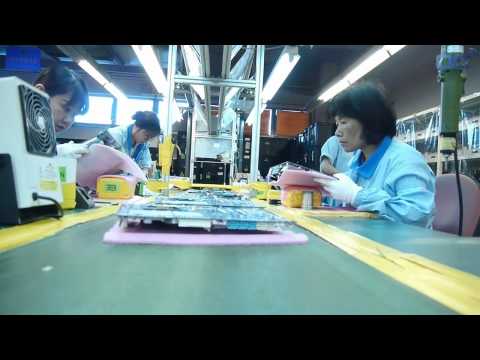
如何製作主機板?技嘉工廠導覽影片大公開! (How to make a Motherboard - A GIGABYTE Factory Tour Video)
0
Peter Yang 發佈於 2021 年 01 月 14 日好奇主機板是怎麼做出來的嗎?這支由 Overclocking TV 帶來的 Gigabyte 工廠導覽,將帶你深入了解 PCB 組裝流程,實際看看表面黏著元件(SMD)是如何被精準放置和焊接的!透過影片,你將學到許多電腦硬體製造的進階詞彙,是個能同時學習新知、提升英文聽力與詞彙量的絕佳機會喔。
在 APP 上學習此影片!
在 VoiceTube App 中有針對影片更深入的練習方式唷!